- Introduction
In power semiconductor industry, Silicon Carbide (SiC) based devices become a prominent alternative in compared to Silicon (Si) based device due to its superior characteristics. For example, in the term of power dissipation; high voltage blocking capability due to high breakdown electrical field- 4×10⁶V/cm, high electron drift velocity – 2×107cm/s, high thermal conductivity – 4.9W/cm-°K, large bandgap energy leads to higher temperature operation capability, higher radiation hardness, and relatively higher thermal conductivity. Recently, the mobile communication systems have seen a fast development in which high-frequency power transistors are required by the base stations. In fact, in the satellite communication and Military Radar field; traveling wave tube and magnetrons are been replace by high-power transistors due to a compact size, low weight, and long life of the transistor. Thus, silicon carbide (SiC) device becomes more attracting in the market.
Silicon carbide (SiC) devices can work under such an outrageous condition that it is required to empower critical upgrades to a far-extending assortment of applications and systems. Silicon carbide (SiC) devices are used in high-temperature, high-power, and highly radiated condition. These devices improve the high voltage switching for efficient power distribution, to drive powerful microwave electronics for military radar and communication, and controls the fuel or engine of aircraft and automobile for higher efficiency. In compared to the silicon carbide (SiC) devices, the other semiconductors are not able to perform under extreme condition [1-2].
In addition, the reverse recovery time is the effect of recombination and sweep out of holes and electrons. The reverse recovery time of silicon carbide (SiC) device totally depends on the internal device parameters and the external operating conditions. The internal parameters are related to a manufacturing process. But the external parameters are the turn-off voltage, forward current, commuting di/dt, and junction temperature. This parameter is used to analyze the performance of the silicon carbide (SiC) devices. At high junction temperature, the turn-off voltage performance of the Silicon carbide (SiC) devices get worse but in compared to silicon (Si) devices, it’s much better. Silicon carbide (SiC) devices can work at high temperature at 200oC. The feature of Silicon carbide (SiC) devices like wide bandgap energy, high thermal conductivity, and high dielectric breakdown which improve the reverse recovery time.
The Silicon Carbide (SiC) devices have specific on-resistance (Ron). The on-resistance (Ron) of the device rise when current flows through parasitic body diodes for mass production. Due to the parasitic body diodes, the base planes are dislocated, induce expansion of stacking faults in 4H-SiC epilayers. The on-resistance (Ron) and drain to source resistance of silicon carbide (SiC) devices have the effects like self-heating, channel length modulation and temperature effects on the parameters as mobility. The main reason behind the on-resistance (Ron) is not only the active area of the silicon power die. But the bonding wire configuration and top metallization debiasing effects have equal importance. Two of the conventional MESFET device are compared. The constant current from the drain to source is 8Amp. The die size is 13.2mm2 and the active area is 10mm2. The blocking voltage is 1200Volt. The typical on-resistance (Ron) is 0.09
n = integer = 1 for the existing ground state.
This type of inconsistency happens between the actual binding energy (59 meV) and the effective mass. The improved voltage of the central cell is approx. 53 meV. The large central cell correction which have wave function create defects like much more localization. If the number of correction increase than the more localization increase in wave function. In fact, the interaction among the core and central cell is more. This is the main reason that the P0 line is shorter than Q0 line in the spectrum. The electric photoluminescence is not limited to silicon carbide. In silicon carbide (SiC), the ratio of the bound excitons luminescence and the free electrons provide accurate doping level [31].
Complex assessment task? We know exactly what markers reward.
Our assessment specialists decode your marking rubric and produce model answers that hit distinction criteria — for written, practical, and portfolio tasks at universities across the US, UK, Australia, Canada, UAE, and Kuwait.
✓ Plagiarism-free · ✓ 100% human · ✓ Free revisions · ✓ Confidential
🔒 No payment to start · From 3 hrs
Since the defects of nitrogen in cubic site is less than the correction of the central cell. In pure crystal, the absorption of the bandgap photons can create hole-electron pairs, and this bandgap photon binds the free excitons. Thus, freely moving in the crystal state is possible until the recombination occur. If similar process for some part of nitrogen is required than there is need to have free excitons. The free excitons of some part of nitrogen will lose the energy and after all this it try to bind with the center that have four-particle known as the bound excitons. This four-particle can form electron-hole pair.
- Properties of Silicon Carbide (SiC).
- Crystal Structure.
In the fourth column of periodic table, there are semiconductors materials. The semiconductors materials are the group of materials that are intermediate of metal and insulators in case of conductivities. This material neither they are good conductor nor they are good insulator. The characteristic of this material varies with change in temperature or by adding impurities. Due to wide variation in characteristic helps the electronic device to perform different function.
In recent year, Silicon carbide (SiC) device has capabilities to replace the silicon (Si) device due to the feature like high voltage blocking capability, high temperature operation capability, and a much lower on-resistance in compare to silicon device. Silicon carbide is a crystalline compound of silicon and carbon, and known by carborundum. Its available rarely in the nature in the form of mineral moissanite. Silicon carbide is non-oxide ceramic with properties like high hardness and strength, high melting point, thermal and chemical stability, oxidation resistance, high erosion resistance.
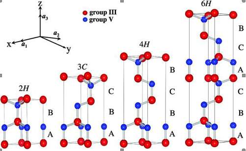
Figure 2.5. The Silicon Carbide (SiC) material structure.
Silicon carbide have more than 200 polytype [40]. Figure 2.5 contains the structure of the silicon carbide. There are three standard structure of silicon carbide 1). Cubic crystal 2). Hexagonal crystal 3). Rhombohedra crystal. The 3C, 4H, 6H and 15R are the common polytype of silicon carbide. The band gap energy of silicon carbide change from 2.3 eV for 3C-SiC to 3.2 eV for 4H-SiC. The silicon carbide hexagonal structures 4H-SiC and 6H-SiC are the polytypes available in bulk wafer. In Silicon carbide, the hexagonal polytypes 6H and 4H have the great capabilities for electronic devices. The main difference among the 6H and 4H is the electron mobility of 6H-SiC is half of the 4H-SiC which is perpendicular to c-axis, and 4H-SiC is 10 times of the that of 6H-SiC parallel to the c-axis [28].
Complex assessment task? We know exactly what markers reward.
Our assessment specialists decode your marking rubric and produce model answers that hit distinction criteria — for written, practical, and portfolio tasks at universities across the US, UK, Australia, Canada, UAE, and Kuwait.
✓ Plagiarism-free · ✓ 100% human · ✓ Free revisions · ✓ Confidential
🔒 No payment to start · From 3 hrs
- 3C-SiC.
One of biggest advantage of the 3C-SiC is that it can be grown on the silicon substrate but it is cheaper quality. In future, the combine integration of 3C-SiC device and the silicon device can be done on the same chip. In compare to 4H-SiC device, the 3C-SiC device has more electrons mobility and less hole mobility. Among all the polytype devices, the 3C-SiC has main drawback that it has low bandgap and low breakdown voltage. Figure 2.6 shows about the structure of the 3C-SiC device. The 3C-SiC beta version is use for the commercial. Presently, the used of the beta form is more as heterogeneous catalysts in compare to the alpha form.
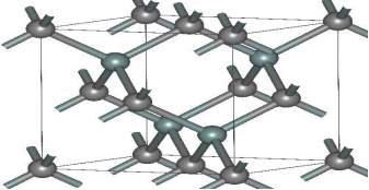
Figure 2.6. The Structure of (β) 3C-SiC.
- 4H-SiC.
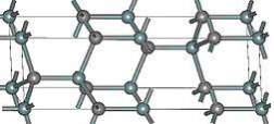
A small anisotropy in which the low field mobility of silicon device is double the 4H-SiC device. The mobility is 20% higher in the parallel direction to c-axis. The anisotropy of the 4H-SiC rest on the electric field, and in the c-axis direction the saturation velocity is 20 % due to high electric field. The 4H-SiC is the mature polytypes which is systematically characterized. At present, the polytype 4H-SiC having good transport properties due this its more favorable in commercial products. Figure 2.7 display the 4H-SiC crystal structure.
Complex assessment task? We know exactly what markers reward.
Our assessment specialists decode your marking rubric and produce model answers that hit distinction criteria — for written, practical, and portfolio tasks at universities across the US, UK, Australia, Canada, UAE, and Kuwait.
✓ Plagiarism-free · ✓ 100% human · ✓ Free revisions · ✓ Confidential
🔒 No payment to start · From 3 hrs
Figure 2.7. The Structure of 4H-SiC.
- 6H-SiC.
In 6H-SiC crystallographic lattice, the long repetition cause the large anisotropy. The mobility in 6H-SiC 25% in the perpendicular direction to the c-axis, and in parallel direction 7% respectively in compare Silicon (Si). Moreover, in 6H-SiC the saturation velocity is 0.2107 cm/s in perpendicular direction to the c-axis and 0.6107 cm/s in parallel direction. The figure 2.8 shows 6H-SiC crystal structure.
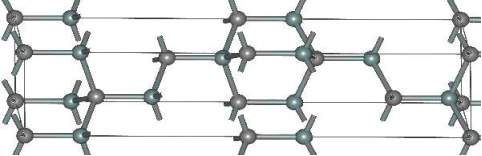
Figure 2.8. The Structure of 6H-SiC.
- Characteristics of Silicon Carbide (SiC).
In all the semiconductors, in compare silicon carbide (SiC) has more wide band gap. This means it’s not temperature sensitive. The advantage of the wide band gap is tolerance to high-temperature, more speed due to high-frequency and high-power due good I-V characteristic.
The fundamental properties of silicon carbide (SiC) polytypes and the silicon (Si) semiconductor is given in Table 1. In Table 2 display about the semiconductor material properties.
Complex assessment task? We know exactly what markers reward.
Our assessment specialists decode your marking rubric and produce model answers that hit distinction criteria — for written, practical, and portfolio tasks at universities across the US, UK, Australia, Canada, UAE, and Kuwait.
✓ Plagiarism-free · ✓ 100% human · ✓ Free revisions · ✓ Confidential
🔒 No payment to start · From 3 hrs
| Quantity | 3C-SiC | 4H-SiC | 6H-SiC | Silicon |
| Thermal conductivity |